04-Sequential_Logic_Design
I Introduction
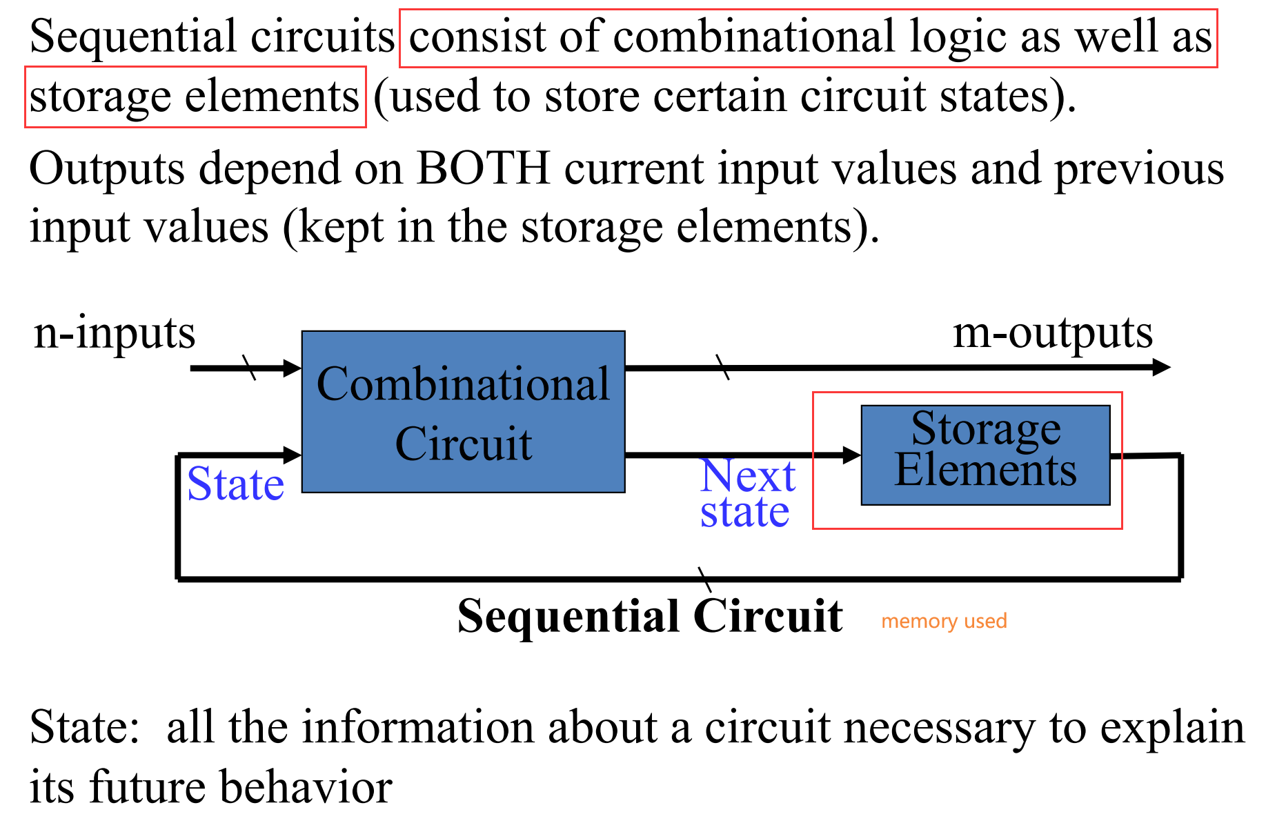
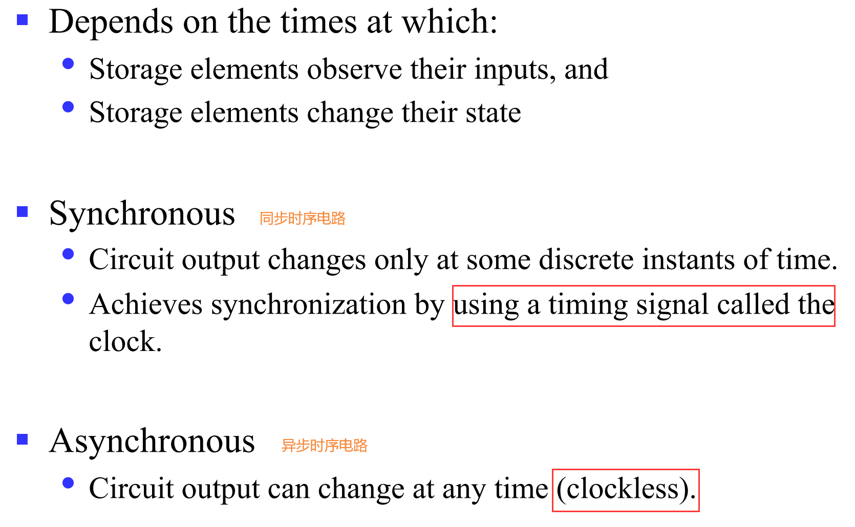
I.1 Trigger
- Level-triggered/sensitive
- Output controlled by the level of the clock input.
- Edge-triggered/sensitive
- Output changes only at the point in time when the clock changes from value to the other.
- Can be positive-edge triggered (0 to 1), or negative-edge triggered (1 to 0).
Flip-flops(触发器) are edge-triggered while clocked (gated) latches(锁存器) are level-sensitive.
I.2 Implement
I.3 Types of Sequential Circuits
II Analysis
II.1 Finite State Machine
Finite state machine (FSM) is a generic model for sequential circuits used in sequential circuit design
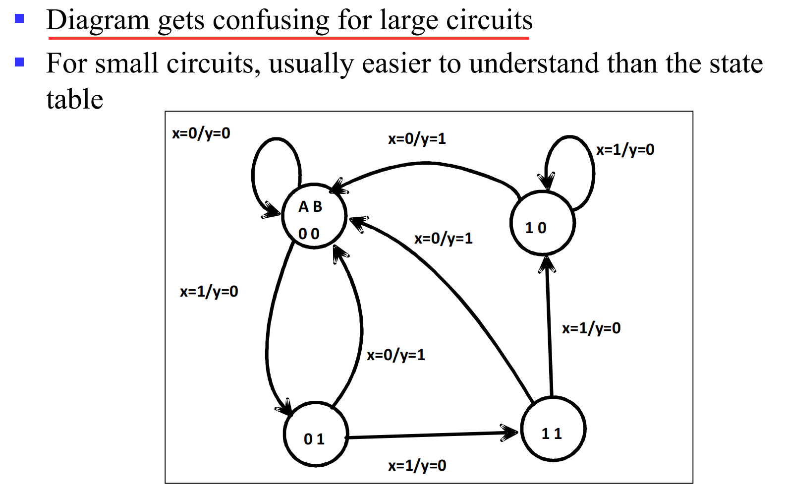
II.1.1 State Diagram
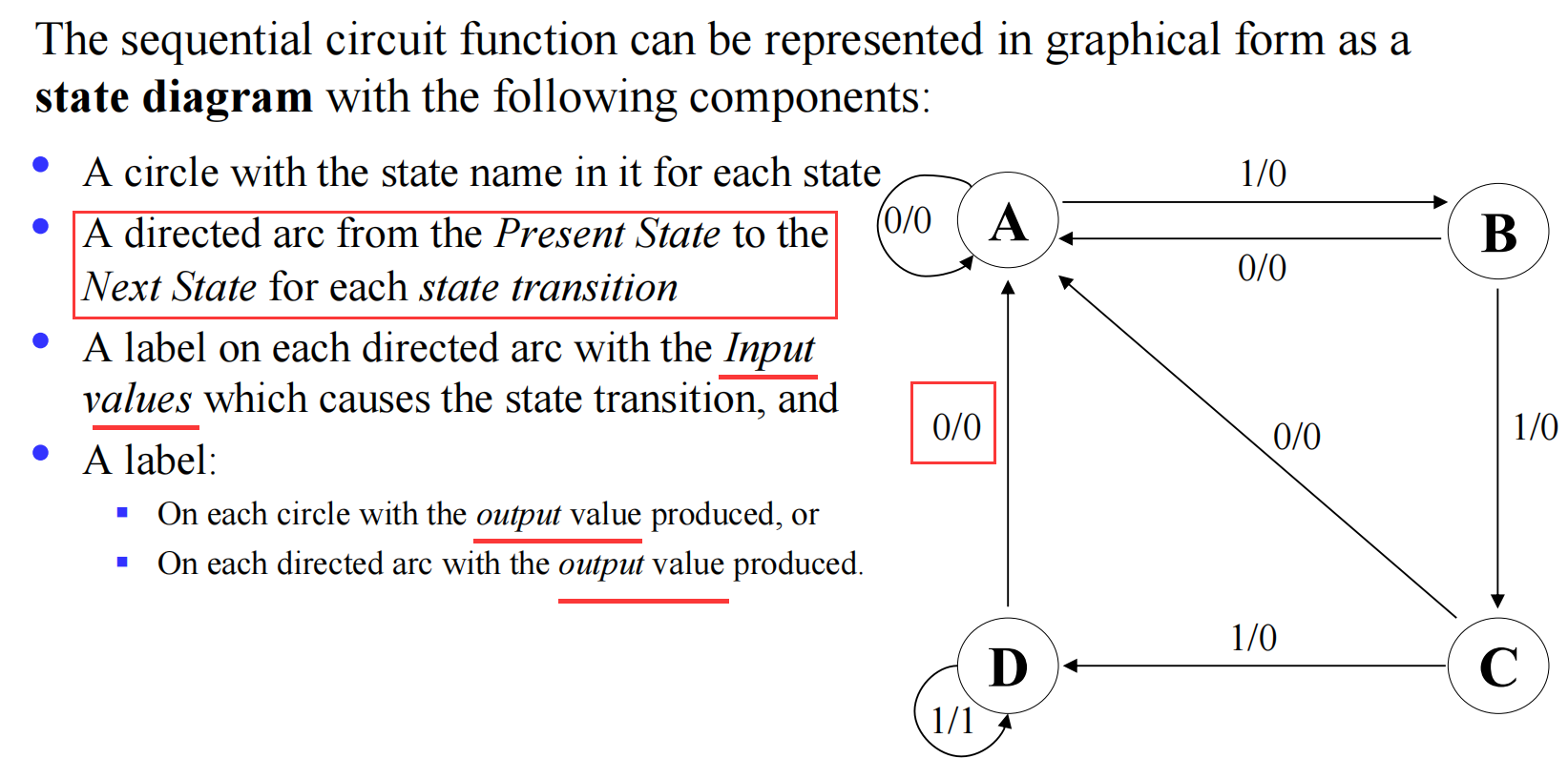
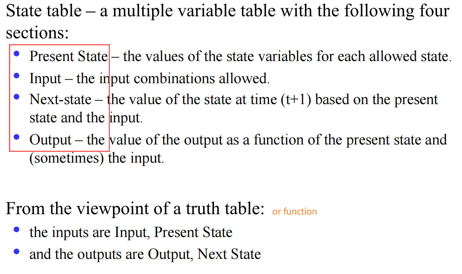
II.1.2 State Table
II.2 Basic Analysis Procedure
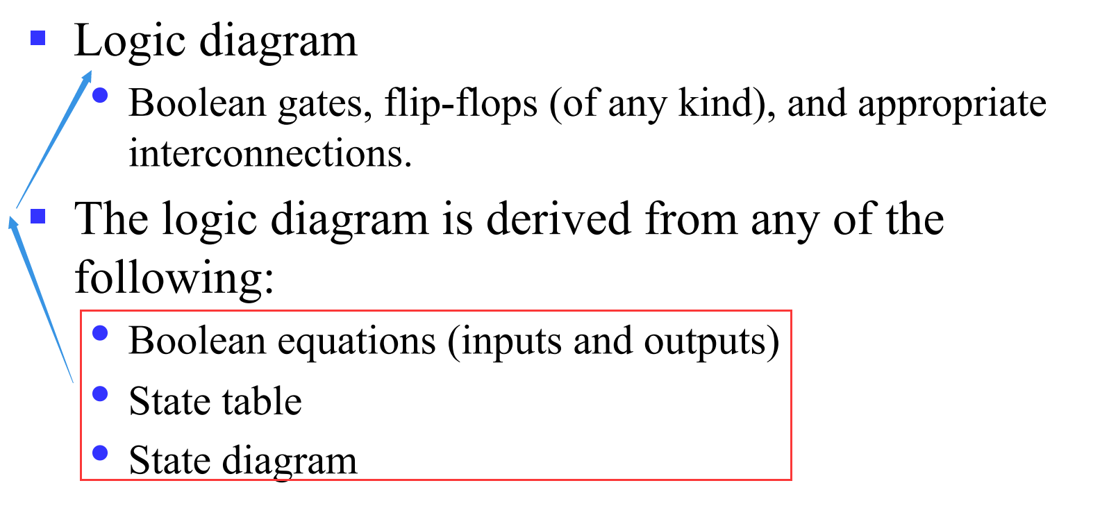
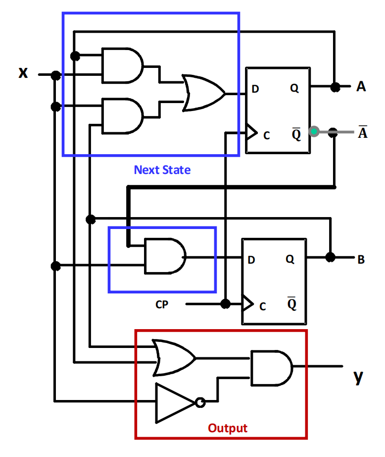
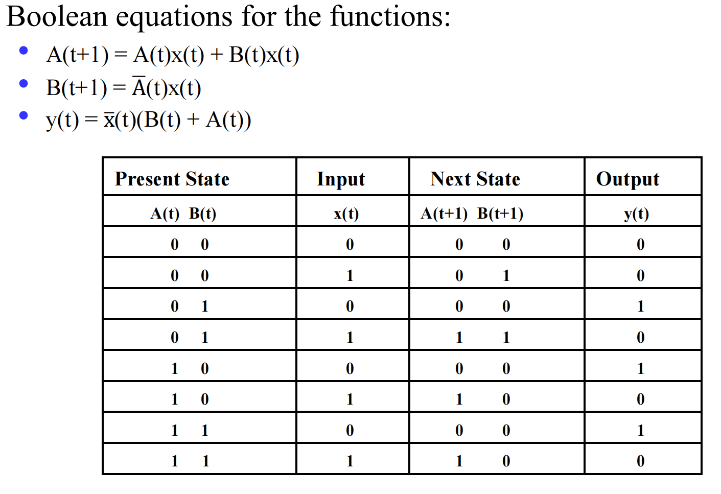
The analysis consists of obtaining a suitable description that demonstrates the time sequence of inputs, outputs, and states.
II.2.1 example
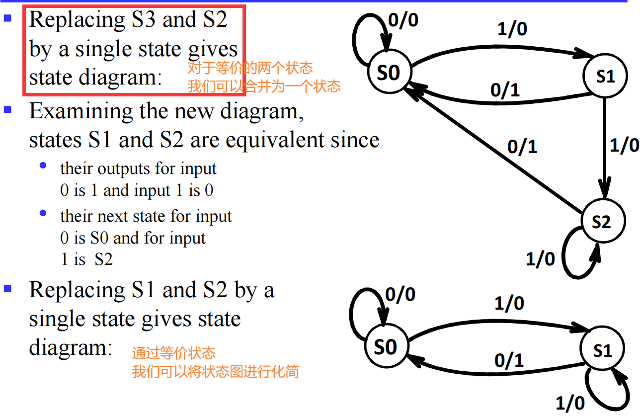
下面所表示的信息是一致的
如何使用 FSM 判断一个二进制数能否被 3 整除?相融关系 R 的迭代算法 的 Example
III Basic sequential logic elements
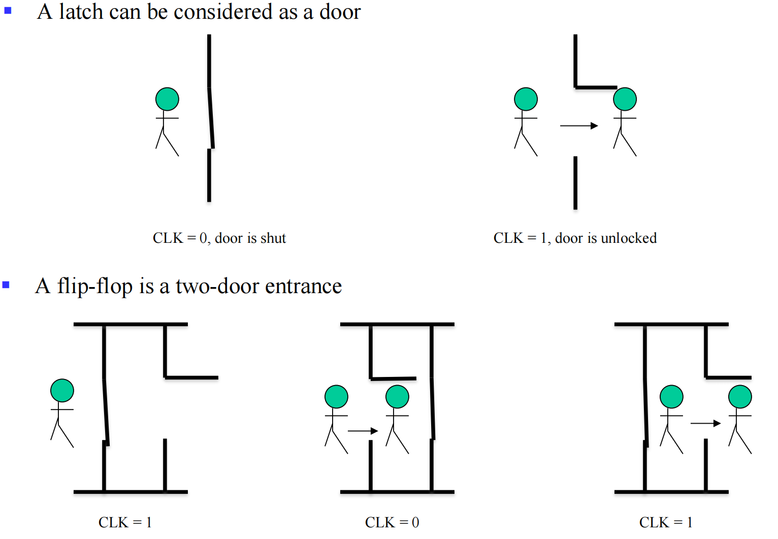
III.1 Latch
双稳态电路(Bistable Circuit)是一种电子电路,它具有两个稳定的状态,并且可以在没有外部影响的情况下无限期地保持在这两个状态之一,直到被触发以改变到另一个状态。双稳态电路在数字电子学中是基本组件,用于存储二进制信息。这两个稳定的状态通常对应于逻辑电平“0”和“1”,在计算和数字通信系统中用作二进制数字。
III.1.1 simple one
下面是最为简单的双稳态电路,该电路没有输入,有两个输出
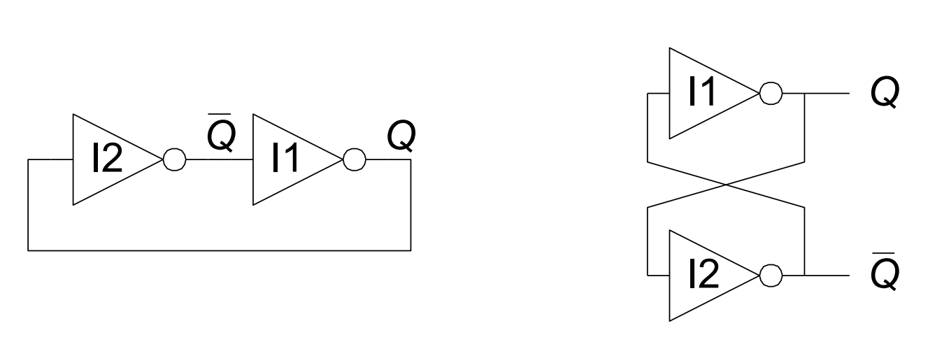
没有输入也就意味着不能够控制该电路
还存在亚稳态(老师上课提了一嘴)
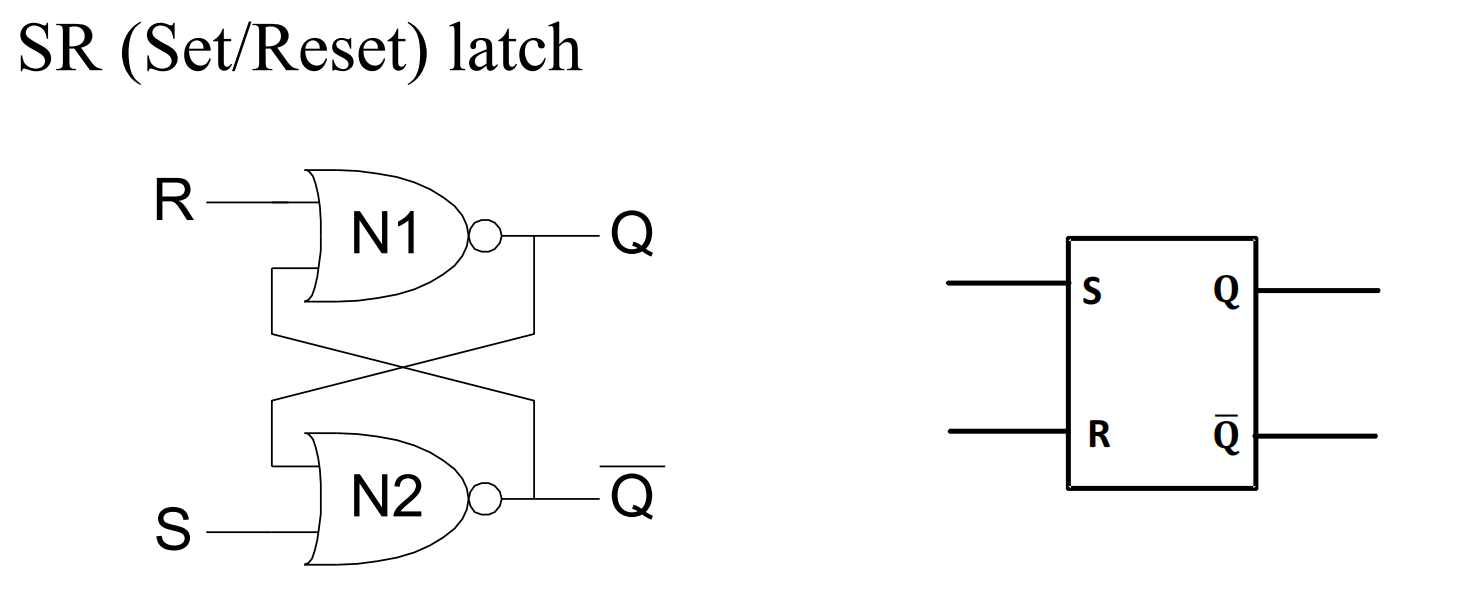
III.1.2 SR Latch
SR Latch:这是最简单的双稳态电路之一,使用 NAND 或 NOR 门创建两个稳定状态:“设置”(Set)和“重置”(Reset)。
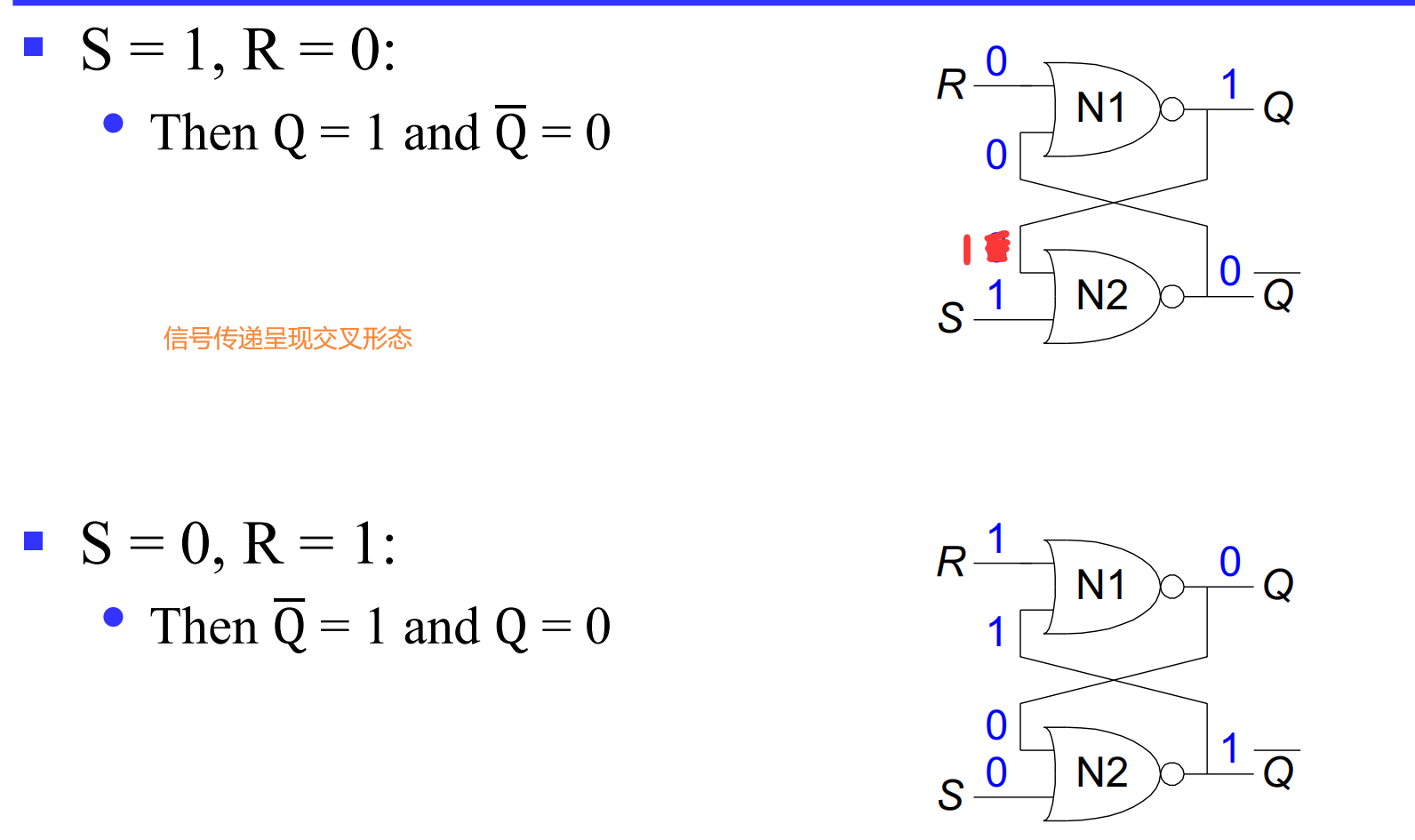
III.1.2.1 analysis
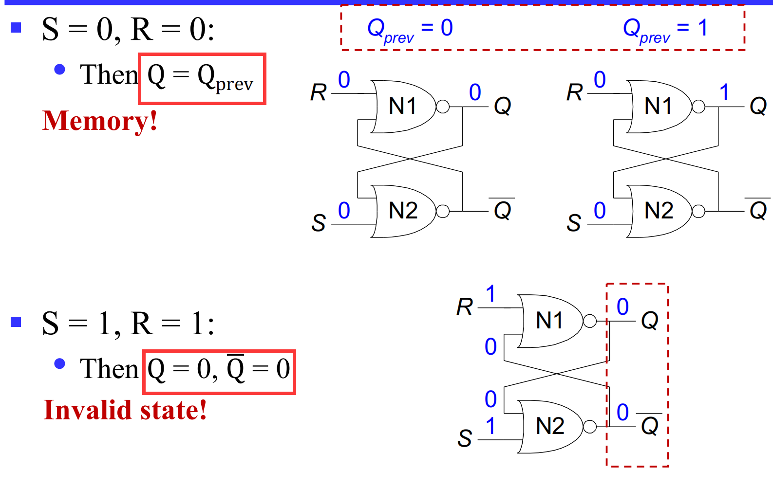
III.1.2.2 summery
III.1.2.2.1 SR Latch with NOR Gates
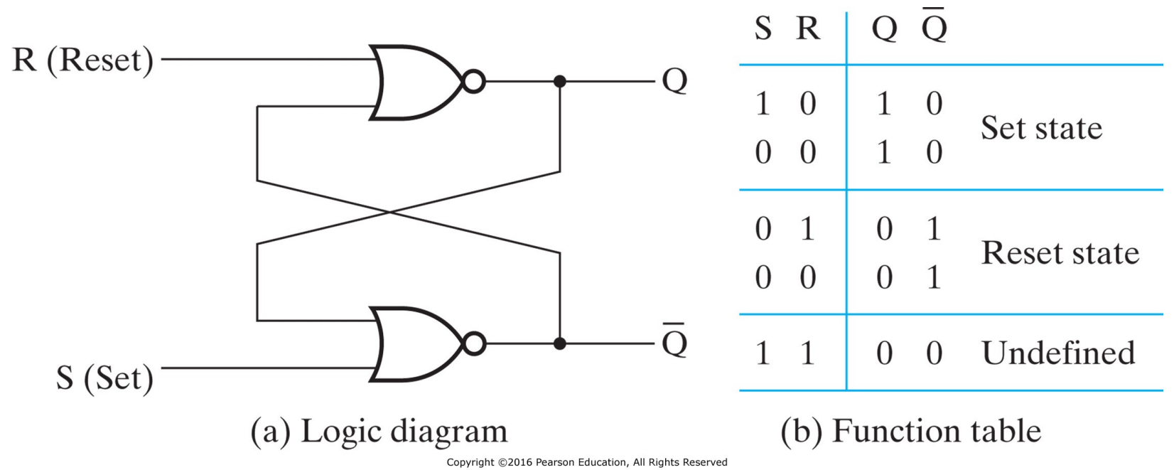
III.1.2.2.2

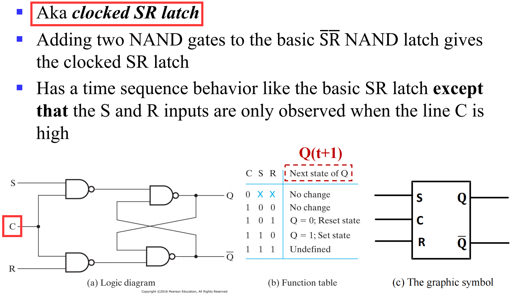
III.1.2.3 SR Latch with Control Input
III.1.3 Latch
在 SR Latch with NOR Gates 中,我们发现不应该出现

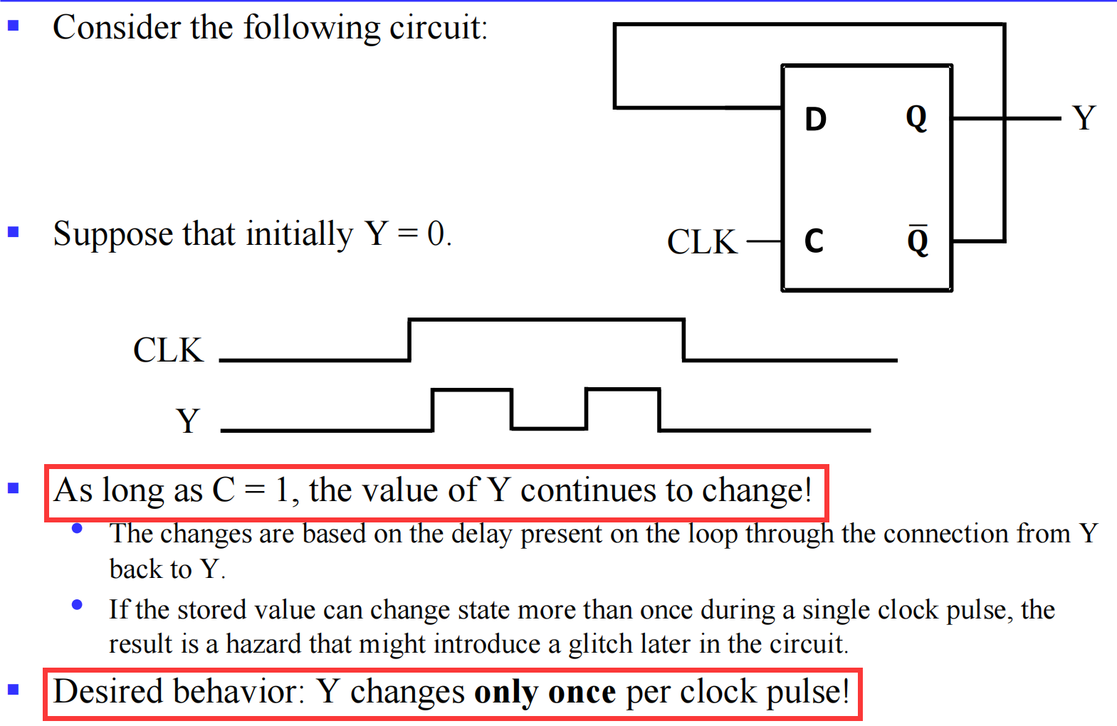
III.1.3.1 The Latch Timing Problem
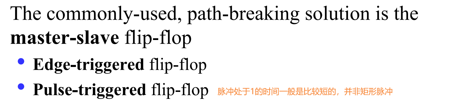
III.2 Flip-Flop
III.2.1 Flip-Flop
III.2.1.1 Implement
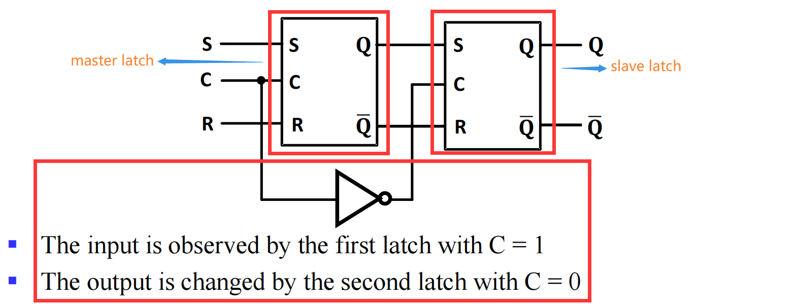
也就是说一定要 C 取 1 后再取 0 信号才能顺利传递;可以看到信号向右传是在 C 由 1 变为 0 的时候发生的,也就是说这是 下降沿触发的 (negative-edge triggered flip-flop)
如何构建上升沿触发?
在最开始的输入 C 取反即可
用 D latch 替换掉 SR latch,触发器就如下:

无疑这是一个上升沿触发型,我们来看看仿真波形图
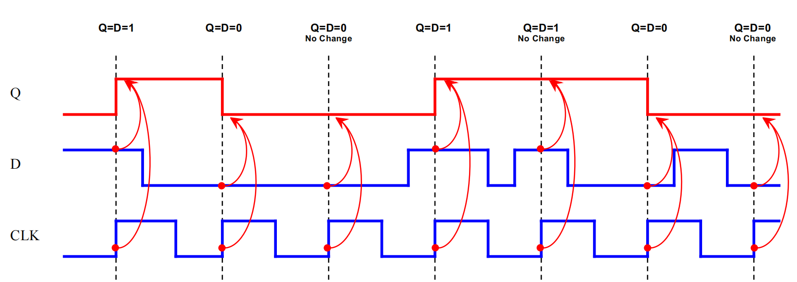
可以看到 Q 的改变发生在两个条件下:
- 时钟上升沿
- D 的值发生了变化
输出只在时钟边沿处根据输入进行 更新
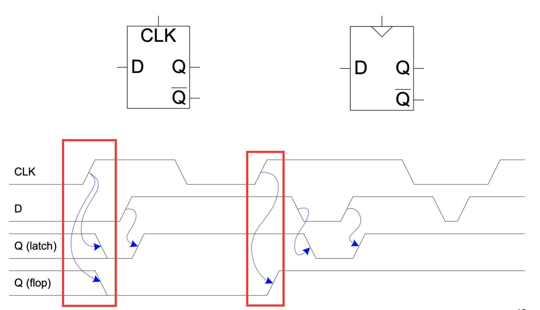
III.2.1.1.1 Latch vs. D Flip-Flop
我们在前面就已经谈到了二者的区别
我们可以通过仿真波形图来比较直观地对比二者
III.2.1.1.2 problem
当然依旧存在 问题:
- 延迟高,电路效率低
- (没太搞懂)
解决 办法: 使用 edge-triggering flip-flop
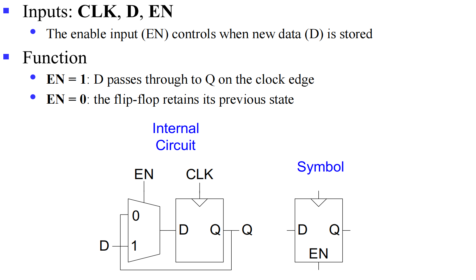
III.2.1.2 Enabled D Flip-Flop
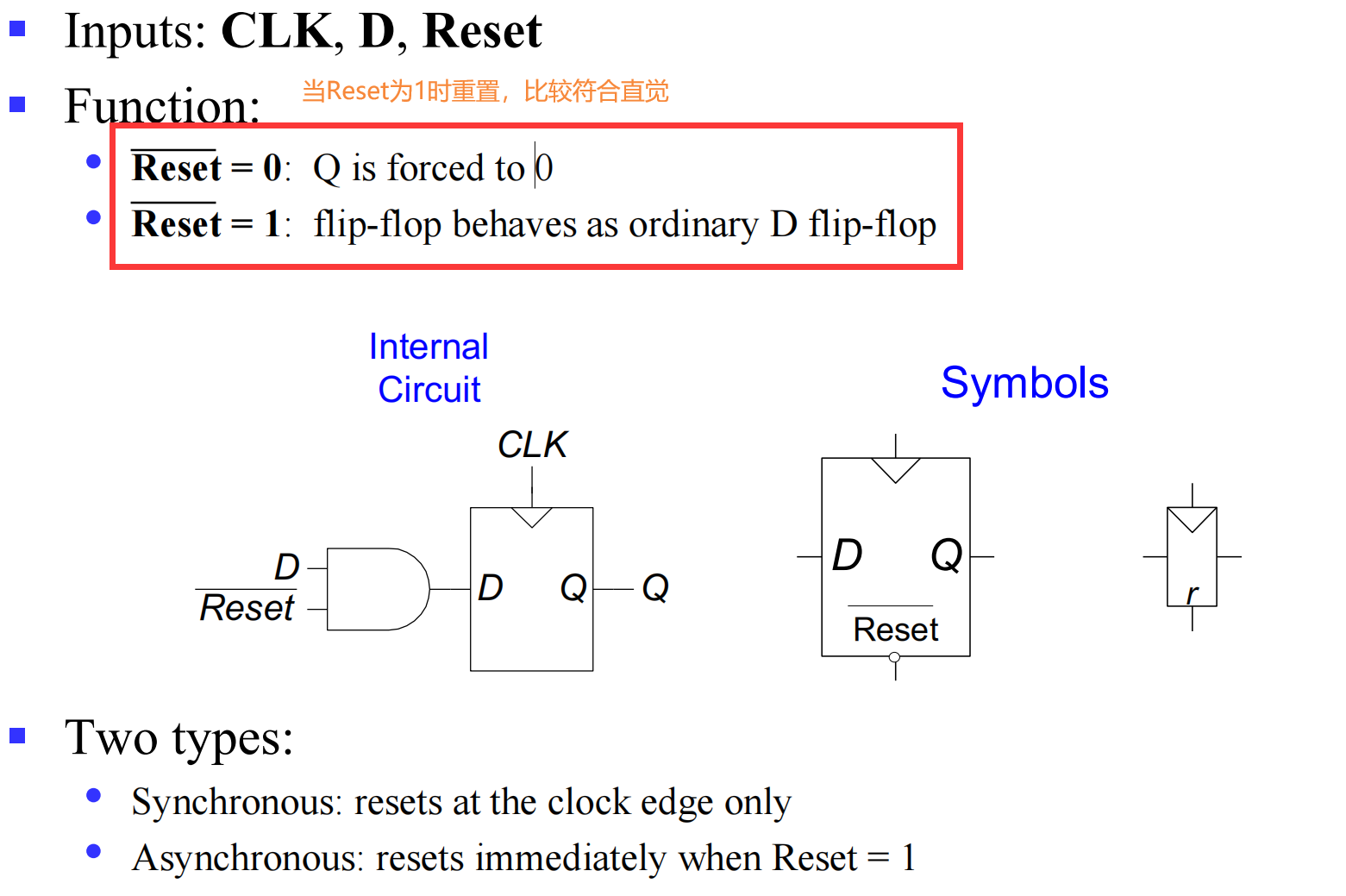
III.2.1.3 Resettable D Flip-Flop
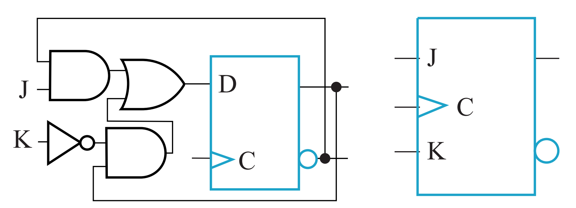
III.2.2 JK Flip-Flop
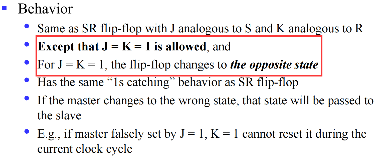
III.2.2.1 Implement
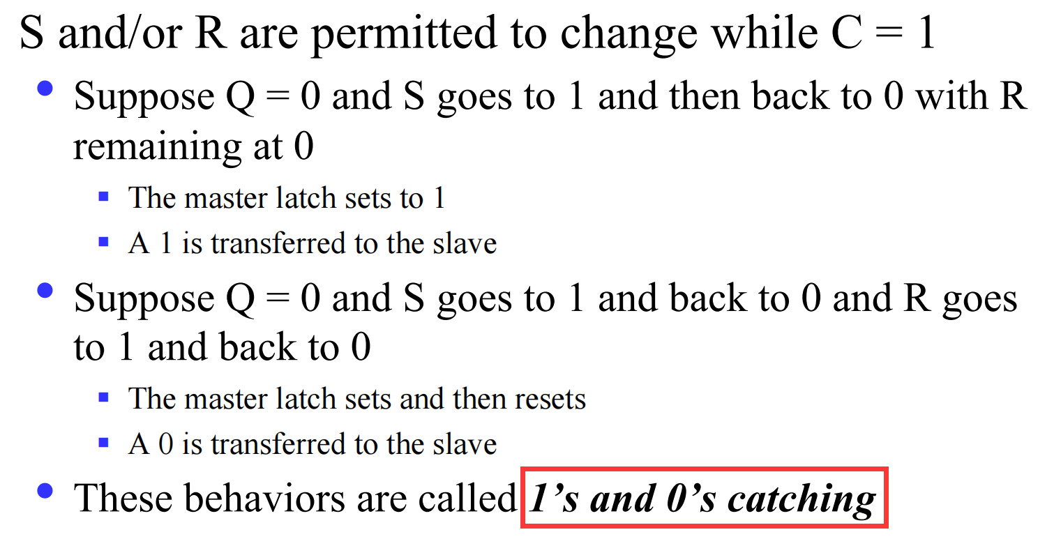
To avoid 1’s catching behavior, one solution used is to use an edge-triggered D as the core of the flip-flop
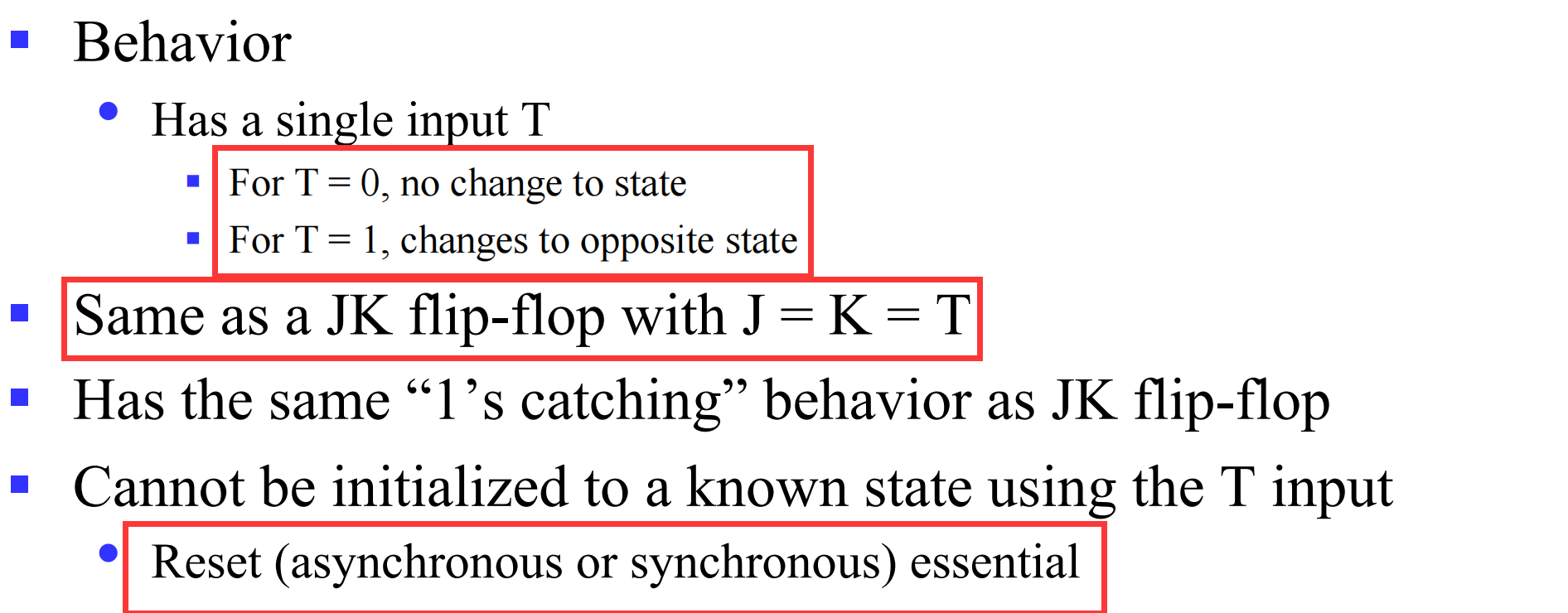
III.2.3 T Flip-Flop
IV Sequential logic design
IV.1 Some definitions
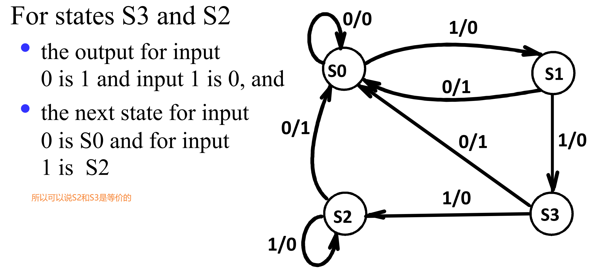
IV.1.1 Equivalent State
- Two states are equivalent if their response for each possible input sequence is an identical output sequence.
- Alternatively, two states are equivalent if their outputs produced for each input symbol is identical and their next states for each input symbol are the same or equivalent.
其实有递归定义的味道;第一点说如果对于任意输入输出相同二者等价;第二点说如果对于任意输入输出的下一状态是等价的,则二者等价
IV.1.1.1 example
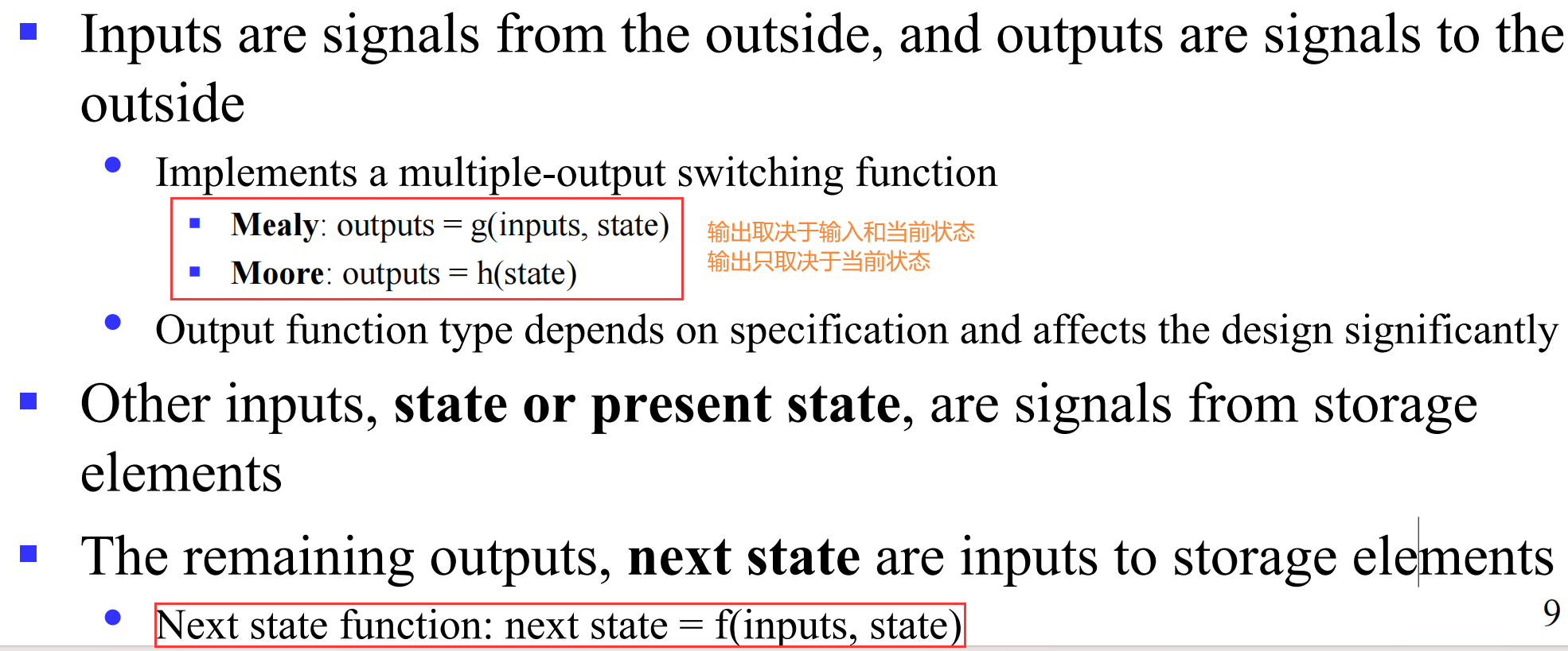
IV.1.2 Moore and Mealy Models
在上面的 Introduction 中我们简单介绍了 Moore and Mealy Models,下面是其一对例子:
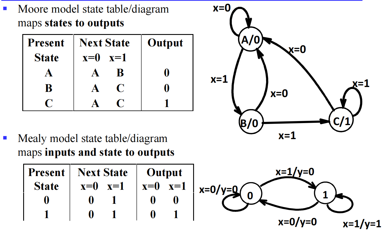
在 Moore 中,输出只受当前状态影响,但是下一状态还是可以受到输入的影响
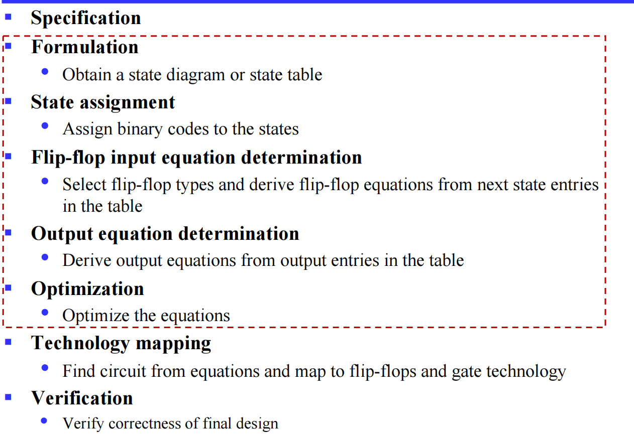
IV.2 The design procedure
到 这里 都直接跳过了,期末再来复习罢
V Classic sequential logic elements
V.1 Registers
V.1.1 Basic introduction
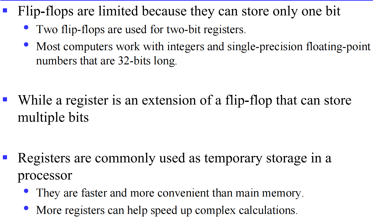
为什么需要寄存器?
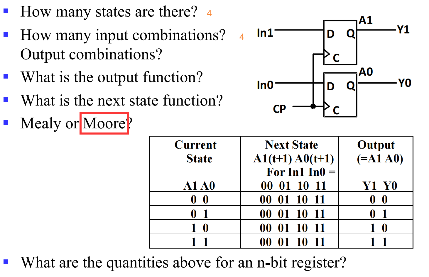
V.1.1.1 2-bit Register
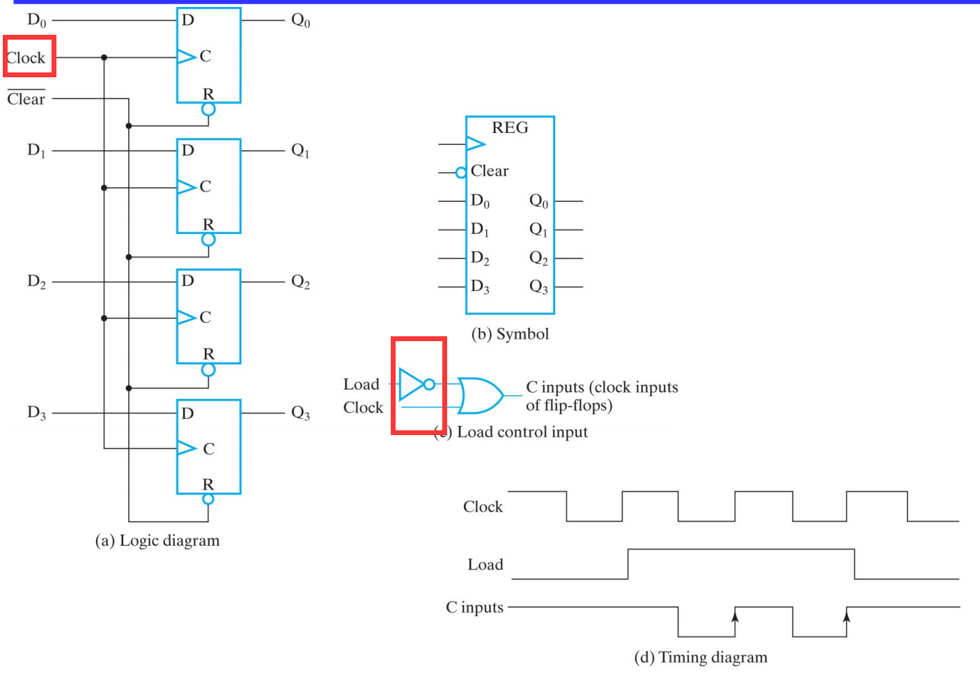
V.1.1.2 4-Bit Register: Clock Gating
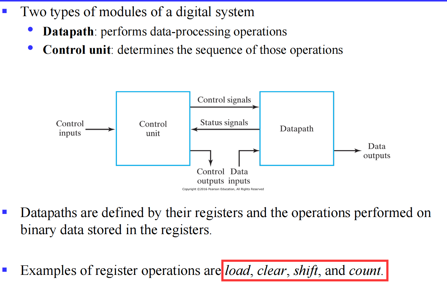
V.1.2 Registers in the digital system
V.1.2.1 Retister Transfers
An elementary operation (such as load, count, add, subtract, and shift) performed on data stored in registers is called a microoperation .
V.1.2.2 Register Representation
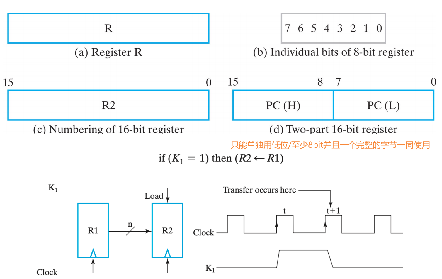
来自 lec04-3 p14,为什么在
下降沿才发生 transfer ?
V.1.2.3 Register Transfer Structures
V.1.2.3.1 overview
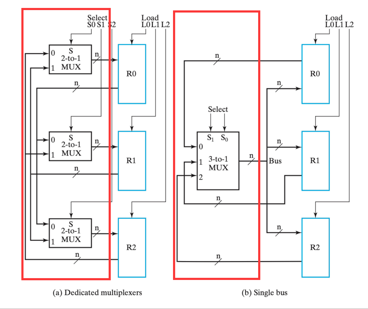
- Multiplexer-Based Transfers - Multiple inputs are selected by a multiplexer dedicated to the register, e.g.,
- Shift registers
- Counters
- Bus-Based Transfers - Multiple inputs are selected by a shared multiplexer driving a bus that feeds inputs to multiple registers
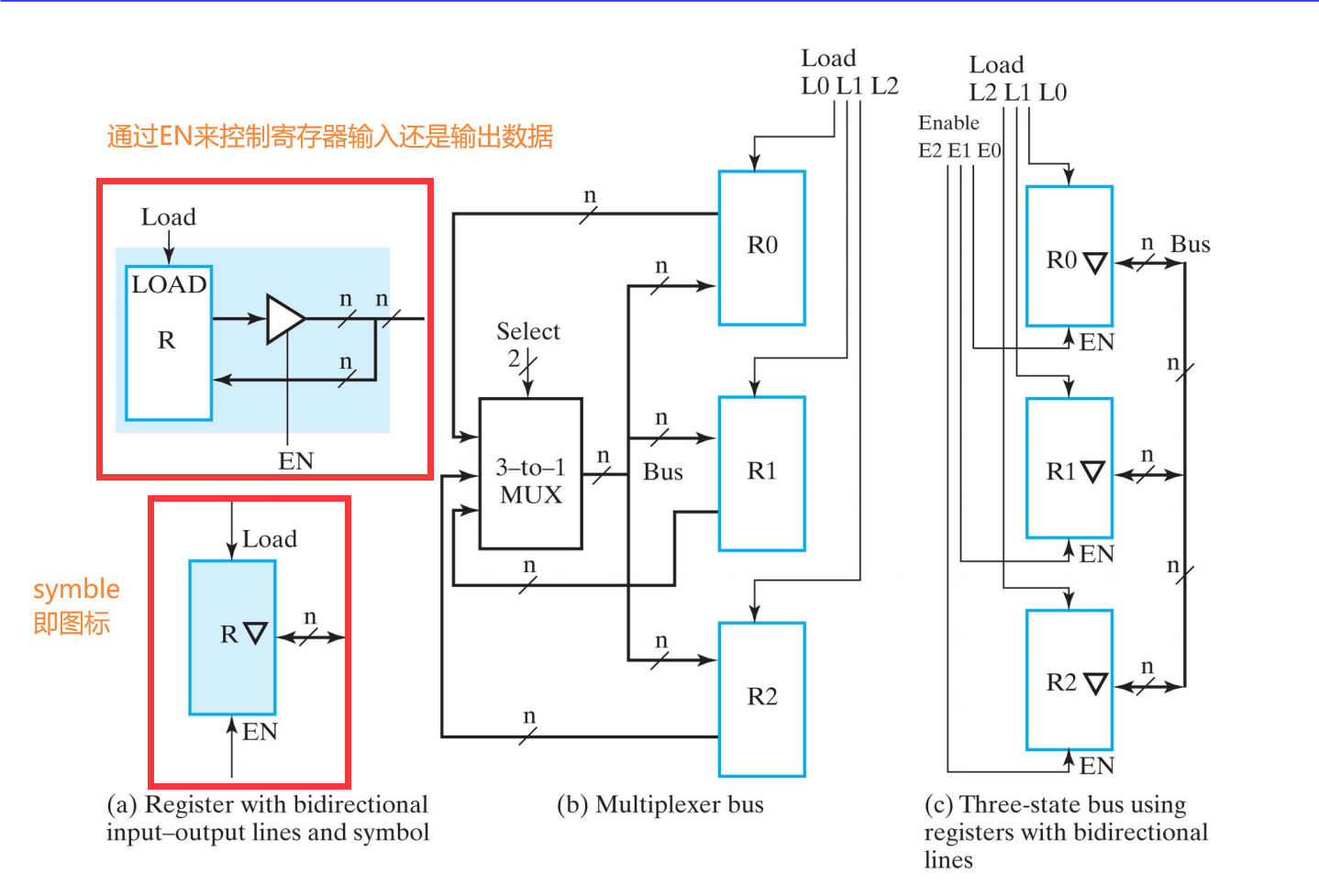
- Three-State Bus - Multiple inputs are selected by 3-state drivers with outputs connected to a bus that feeds multiple registers
- Other Transfer Structures - Use multiple multiplexers, multiple buses, and combinations of all the above
V.1.2.3.2 Dedicated Multiplexers vs. Single Bus
V.1.2.3.3 Multiplexer Bus vs. 3-State Bus
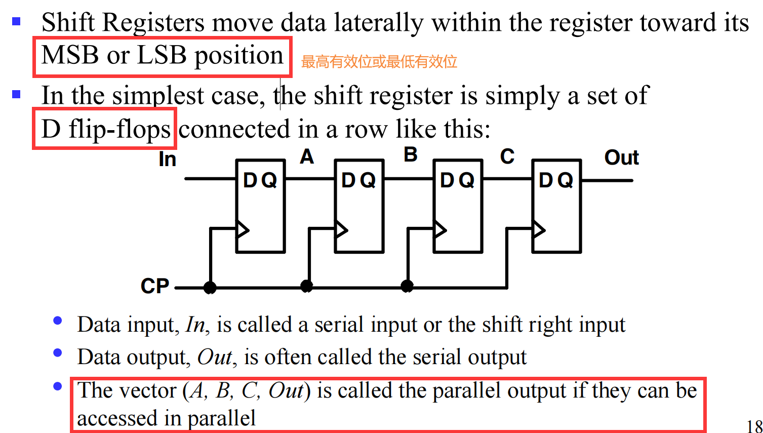
V.1.3 Shift Registers
A register capable of shifting its stored bits laterally in one or both directions is called a shift register
V.1.3.1 Shift Register with Parallel Load
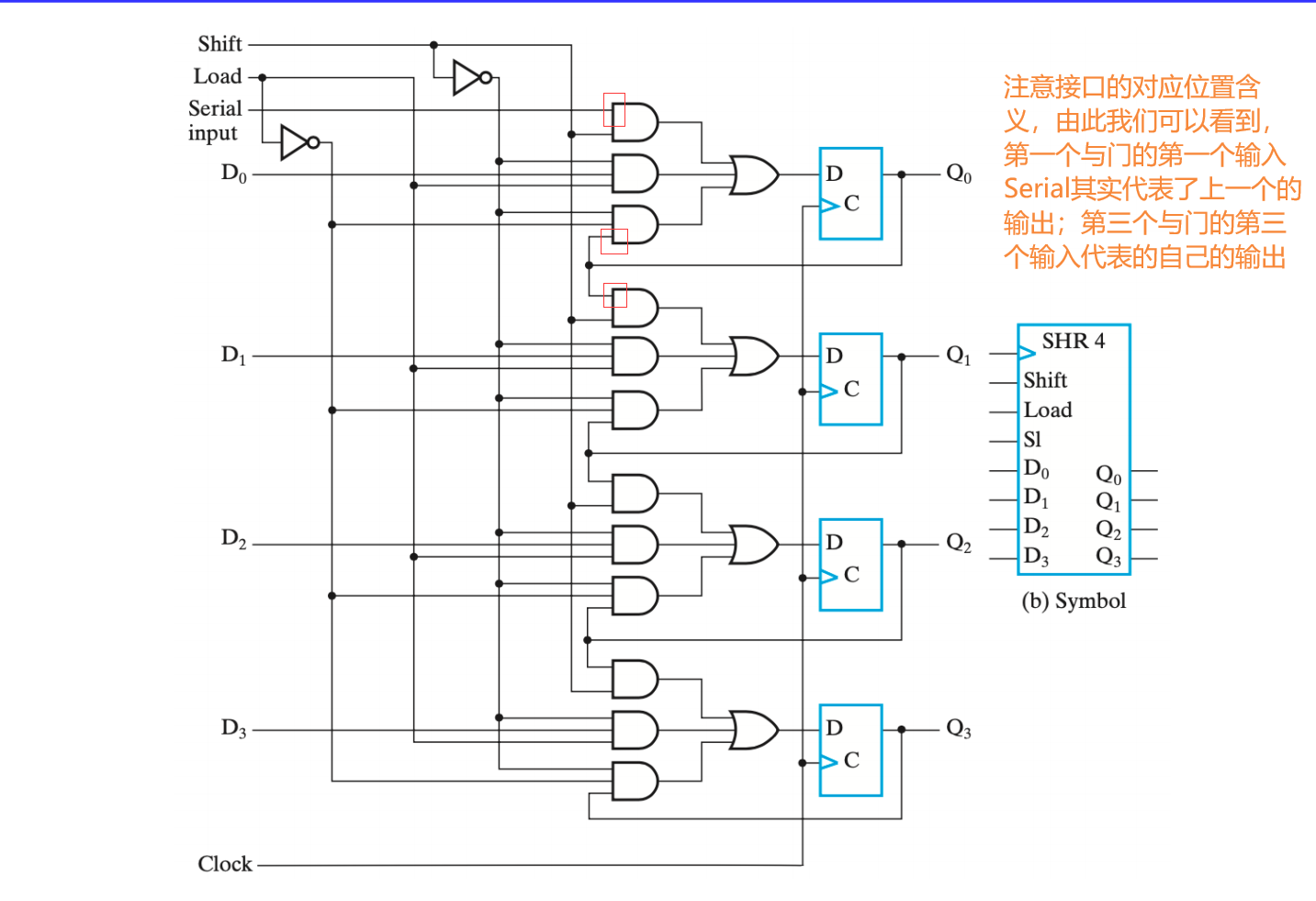
以第一个或门对应的电路部分为例,真值表如下(后面有时间再自己画表格):
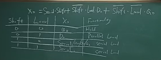
用
- hold 表示保持值不变
- parallel load 表示成功将数值直接放入对应寄存器中
- serial load 表示将上一个的数值放入对应寄存器中,从而实现了 移位 的目的
V.2 Counters
V.2.1 Basic introduction
Counters are sequential circuits which "count" through a specific state sequence. They can count up, count down, or count through other fixed sequences.
All processors contain a program counter, or PC.
- Programs consist of a list of instructions that are to be executed one after another (for the most part).
- The PC keeps track of the instruction currently being executed.
- The PC increments once on each clock cycle, and the next program instruction is then executed.
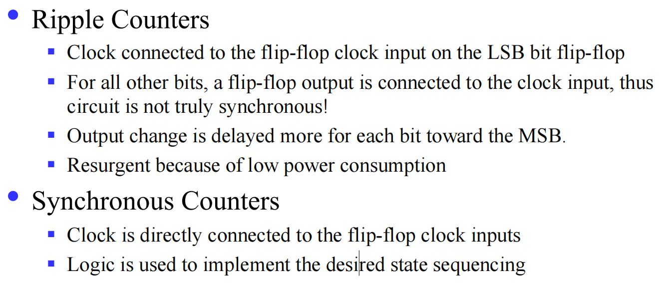
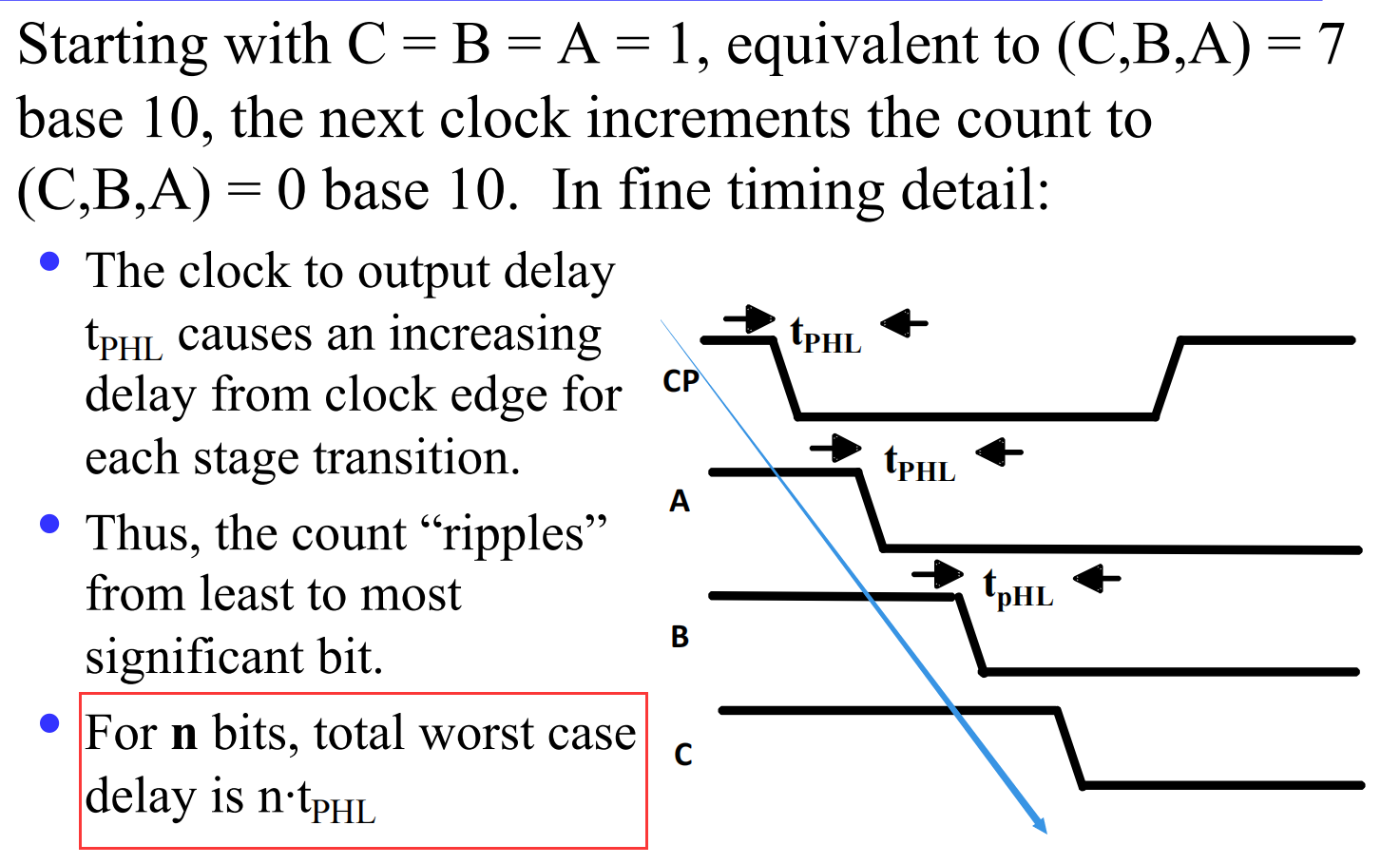
V.2.2 Ripple Counters
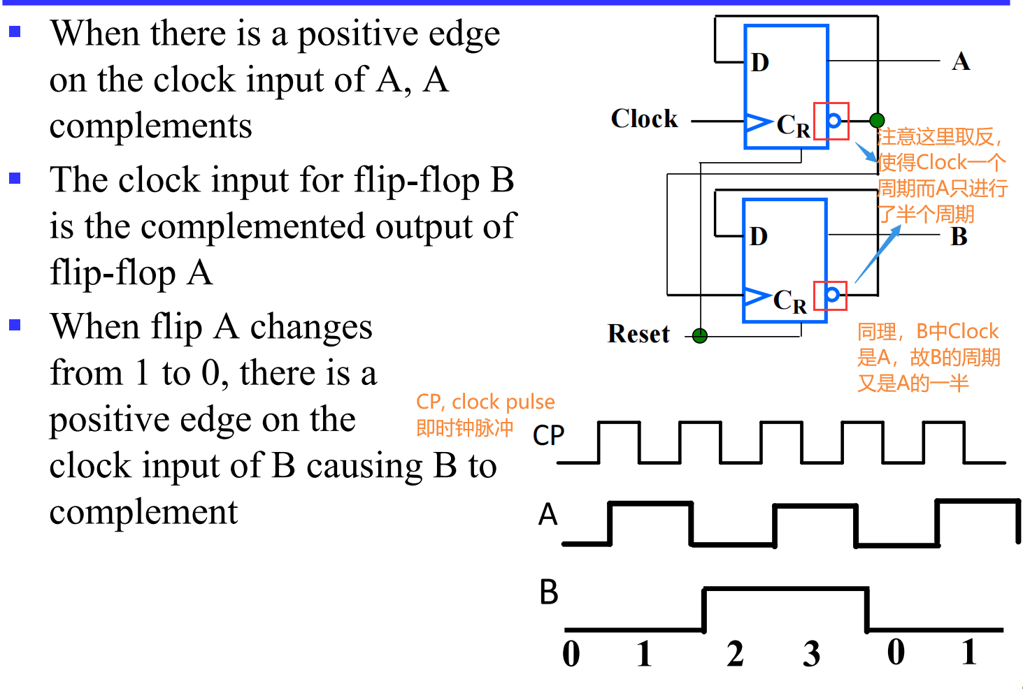
为什么叫行波计数器(ripple counter) ?
These circuits are called ripple counters because each edge sensitive transition (positive in the example) causes a change in the next flip-flop’s state.
考虑信号变换用时,我们可以更加直观地来理解:
实验指导——分频器
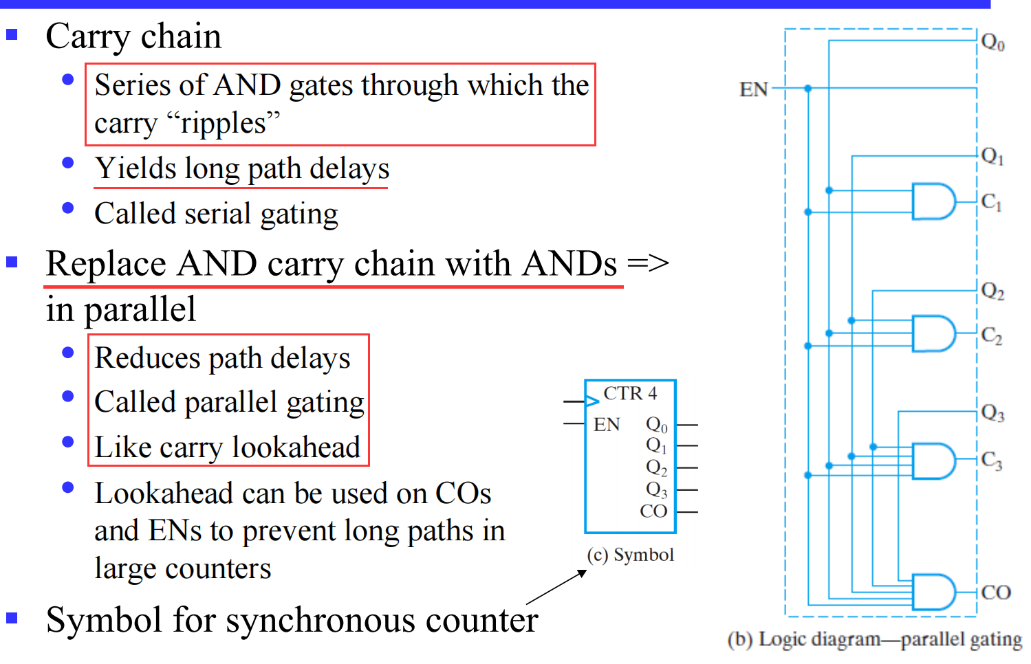
V.2.3 Synchronous Counters
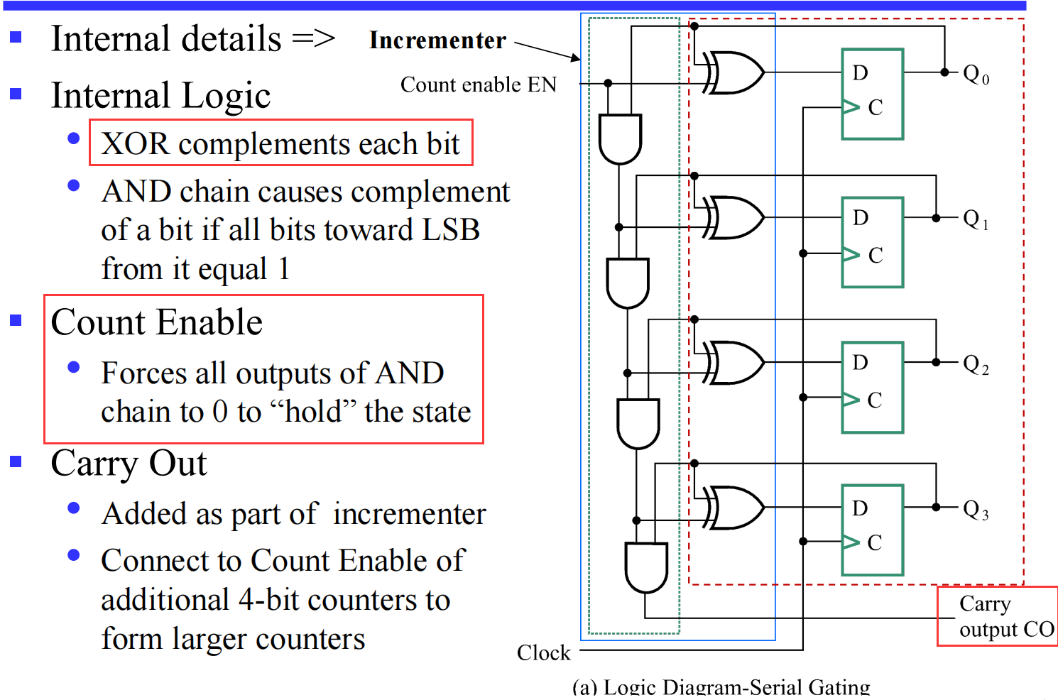
实现进位/计数的原理?
[!HINT]
课堂录播 (54:27开始)
一连串的与门我们需要的计数较大时产生极大的延迟,这对于计数是不利的;仿照 Shift Register with Parallel Load ,我们将 counter 写为 parallel mode
V.2.4 Other Counters
- Divide-by-n (Modulo n) Counter
- BCD counter with D flip-flops
实验指导——计数器
对于 BCD 在 lec04-3 的 34 页后没看了,如果不懂了再看